
 Download:
Figures of the Article
-
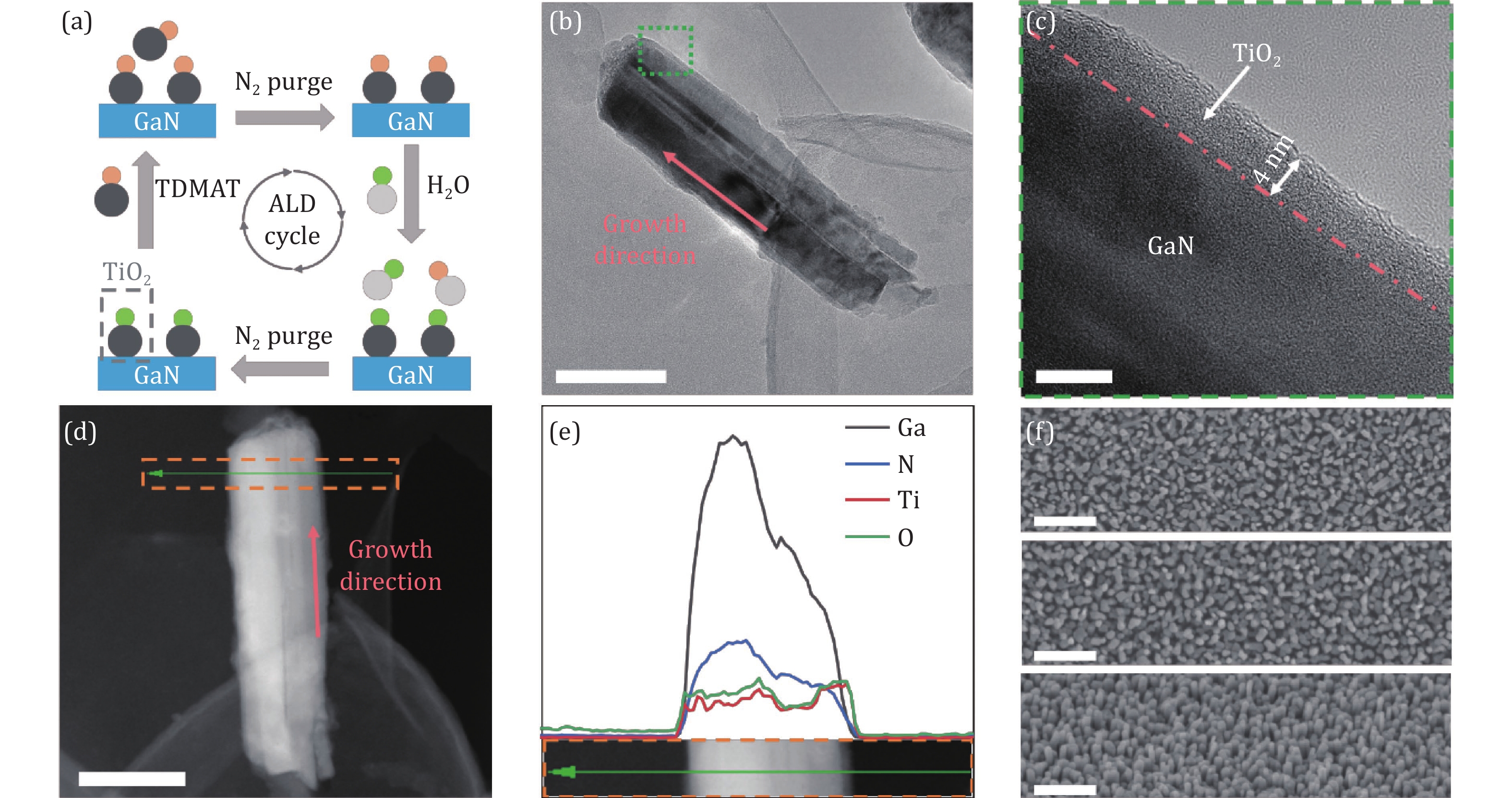
![]() (a) Schematic illustration of ALD decoration process. (b) Overview of the TEM image of GaN@TiO2 nanowire (scale bar, 100 nm). (c) Selected-area TEM image of GaN@TiO2 nanowire (scale bar, 10 nm). (d) STEM image of GaN@TiO2 nanowire (scale bar, 100 nm). (e) EDS line profiles of Ga, N, Ti, and O across the GaN@TiO2 nanowire. (f) Top-view SEM images of GaN nanowires (top; scale bar, 500 nm) and GaN@TiO2 nanowires (middle; scale bar, 500 nm), and side-view SEM image of GaN@TiO2 nanowires (bottom; scale bar, 500 nm).
(a) Schematic illustration of ALD decoration process. (b) Overview of the TEM image of GaN@TiO2 nanowire (scale bar, 100 nm). (c) Selected-area TEM image of GaN@TiO2 nanowire (scale bar, 10 nm). (d) STEM image of GaN@TiO2 nanowire (scale bar, 100 nm). (e) EDS line profiles of Ga, N, Ti, and O across the GaN@TiO2 nanowire. (f) Top-view SEM images of GaN nanowires (top; scale bar, 500 nm) and GaN@TiO2 nanowires (middle; scale bar, 500 nm), and side-view SEM image of GaN@TiO2 nanowires (bottom; scale bar, 500 nm).
-
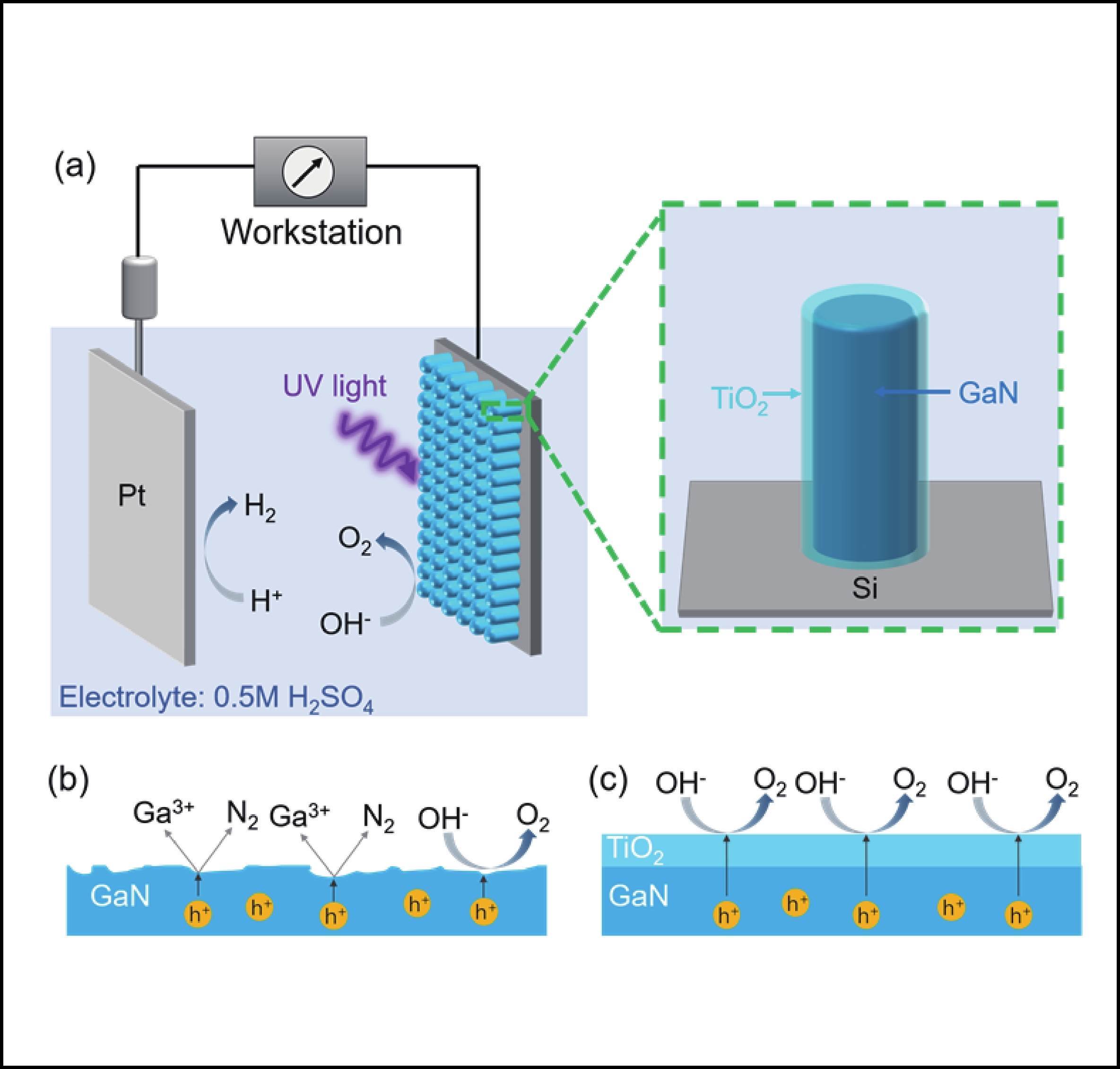
![]() (a) Schematic illustration of the operation of the GaN@TiO2-nanowire-based PEC UV-PDs under UV light irradiation. (b) Bare GaN nanowire surface in which photocorrosion predominates. (c) GaN coated with TiO2 layer, where photogenerated holes can oxidize OH− to O2.
(a) Schematic illustration of the operation of the GaN@TiO2-nanowire-based PEC UV-PDs under UV light irradiation. (b) Bare GaN nanowire surface in which photocorrosion predominates. (c) GaN coated with TiO2 layer, where photogenerated holes can oxidize OH− to O2.
-
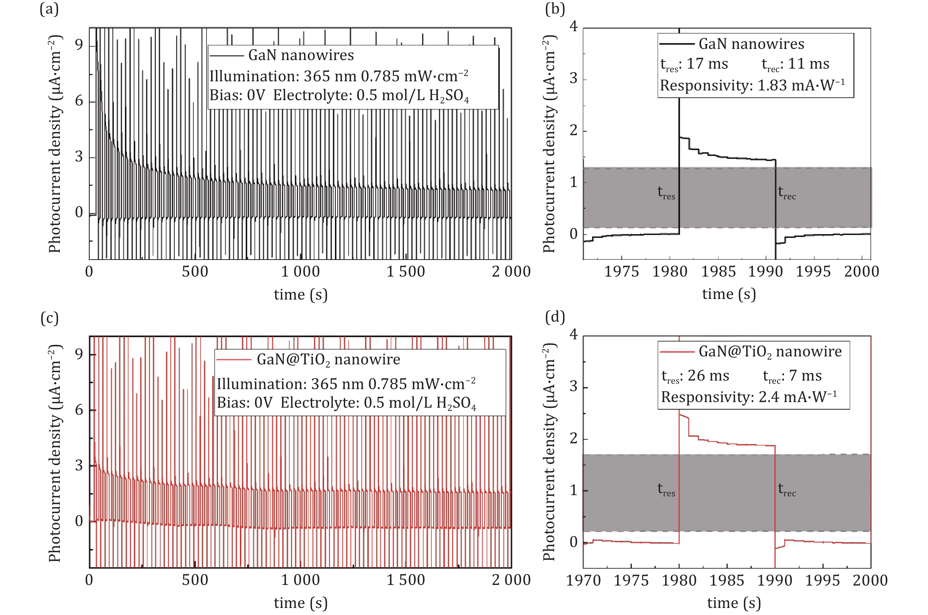
![]() (a) J-t characteristics of GaN-nanowire-based PEC UV-PDs under 365 nm irradiation. (b) Representation of the rise time and decay time interval of GaN-nanowire-based PEC UV-PDs. (c) GaN@TiO2-nanowire-based PEC UV-PDs under 365 nm irradiation. (d) Representation of the rise time and decay time interval of GaN@TiO2-nanowire-based PEC UV-PDs.
(a) J-t characteristics of GaN-nanowire-based PEC UV-PDs under 365 nm irradiation. (b) Representation of the rise time and decay time interval of GaN-nanowire-based PEC UV-PDs. (c) GaN@TiO2-nanowire-based PEC UV-PDs under 365 nm irradiation. (d) Representation of the rise time and decay time interval of GaN@TiO2-nanowire-based PEC UV-PDs.
-
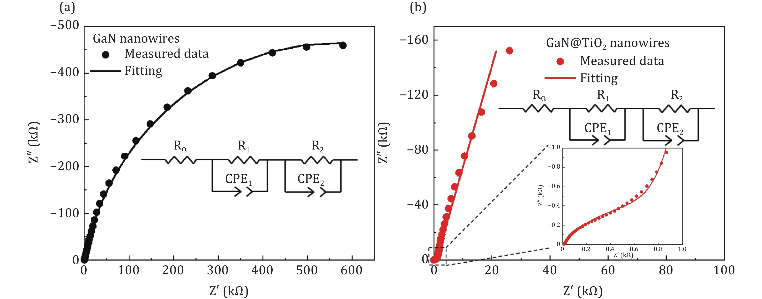
![]() Photoelectrochemical impedance spectra of (a) GaN-nanowire-based and (b) GaN@TiO2-nanowire-based PEC UV-PDs under 365 nm irradiation.
Photoelectrochemical impedance spectra of (a) GaN-nanowire-based and (b) GaN@TiO2-nanowire-based PEC UV-PDs under 365 nm irradiation.
Related articles
-
2024, 54(6): 0605. DOI: 10.52396/JUSTC-2024-0046
-
2022, 52(6): 5-1-5-9. DOI: 10.52396/JUSTC-2021-0258
-
2016, 46(5): 439-448. DOI: 10.3969/j.issn.0253-2778.2016.05.012
-
2013, 43(11): 959-966. DOI: 10.3969/j.issn.0253-2778.2013.11.012
-
2013, 43(5): 402-409. DOI: 10.3969/j.issn.0253-2778.2013.05.008
-
2011, 41(10): 895-901. DOI: 10.3969/j.issn.0253-2778.2011.10.009
-
2010, 40(4): 387-394. DOI: 10.3969/j.issn.0253-2778.2010.04.010
-
2009, 39(7): 755-762.
-
2009, 39(4): 435-439.
-
2009, 39(4): 424-428.
