
| [1] |
Chen J J, Wu K, Hu W, et al. Spin–orbit coupling in 2D semiconductors: a theoretical perspective. J. Phys. Chem. Lett., 2021, 12 (51): 12256–12268. doi: 10.1021/acs.jpclett.1c03662
|
| [2] |
Koo H C, Kim S B, Kim H, et al. Rashba effect in functional spintronic devices. Adv. Mater., 2020, 32 (51): 2002117. doi: 10.1002/adma.202002117
|
| [3] |
Lee S, Koike H, Goto M, et al. Synthetic Rashba spin–orbit system using a silicon metal-oxide semiconductor. Nat. Mater., 2021, 20 (9): 1228–1232. doi: 10.1038/s41563-021-01026-y
|
| [4] |
Lin W, Li L, Doğan F, et al. Interface-based tuning of Rashba spin-orbit interaction in asymmetric oxide heterostructures with 3d electrons. Nat. Commun., 2019, 10 (1): 3052. doi: 10.1038/s41467-019-10961-z
|
| [5] |
Lyu J K, Ji W X, Zhang S F, et al. Strain-tuned topological insulator and Rashba-induced anisotropic momentum-locked Dirac cones in two-dimensional SeTe monolayers. ACS Appl. Mater. Interfaces, 2018, 10 (50): 43962–43969. doi: 10.1021/acsami.8b18582
|
| [6] |
Ciocys S T, Maksimovic N, Analytis J G, et al. Driving ultrafast spin and energy modulation in quantum well states via photo-induced electric fields. npj Quantum Mater., 2022, 7 (1): 79. doi: 10.1038/s41535-022-00490-2
|
| [7] |
Jolie W, Hung T C, Niggli L, et al. Creating tunable quantum corrals on a Rashba surface alloy. ACS Nano, 2022, 16 (3): 4876–4883. doi: 10.1021/acsnano.2c00467
|
| [8] |
Lafalce E, Amerling E, Yu Z G, et al. Rashba splitting in organic–inorganic lead–halide perovskites revealed through two-photon absorption spectroscopy. Nat. Commun., 2022, 13 (1): 483. doi: 10.1038/s41467-022-28127-9
|
| [9] |
Lee S, Kwon Y K. Unveiling giant hidden rashba effects in two-dimensional Si2Bi2. npj 2D Mater. Appl., 2020, 4 (1): 45. doi: 10.1038/s41699-020-00180-2
|
| [10] |
Chen J J, Wu K, Hu W, et al. Tunable Rashba spin splitting in two-dimensional polar perovskites. J. Phys. Chem. Lett., 2021, 12 (7): 1932–1939. doi: 10.1021/acs.jpclett.0c03668
|
| [11] |
Datta S, Das B. Electronic analog of the electro-optic modulator. Appl. Phys. Lett., 1990, 56 (7): 665–667. doi: 10.1063/1.102730
|
| [12] |
Park Y H, Choi J W, Kim H J, et al. Complementary spin transistor using a quantum well channel. Sci. Rep., 2017, 7 (1): 46671. doi: 10.1038/srep46671
|
| [13] |
Chuang P, Ho S C, Smith L W, et al. All-electric all-semiconductor spin field-effect transistors. Nat. Nanotechnol., 2015, 10 (1): 35–39. doi: 10.1038/nnano.2014.296
|
| [14] |
Fu X M, Jia C, Sheng L, et al. Bipolar Rashba semiconductors: a class of nonmagnetic materials for electrical spin manipulation. J. Phys. Chem. Lett., 2023, 14 (50): 11292–11297. doi: 10.1021/acs.jpclett.3c02917
|
| [15] |
Chen J J, Wu K, Hu W, et al. High-throughput inverse design for 2D ferroelectric Rashba semiconductors. J. Am. Chem. Soc., 2022, 144 (43): 20035–20046. doi: 10.1021/jacs.2c08827
|
| [16] |
Song Q, Zhang H R, Su T, et al. Observation of inverse Edelstein effect in Rashba-split 2DEG between SrTiO3 and LaAlO3 at room temperature. Sci. Adv., 2017, 3 (3): e1602312. doi: 10.1126/sciadv.1602312
|
| [17] |
Qu J, Han X, Sakamoto S, et al. Reversal of spin-polarization near the fermi level of the Rashba semiconductor BiTeCl. npj Quantum Mater., 2023, 8 (1): 13. doi: 10.1038/s41535-023-00546-x
|
| [18] |
Nakayama H, Kanno Y, An H, et al. Rashba-Edelstein magnetoresistance in metallic heterostructures. Phys. Rev. Lett., 2016, 117 (11): 116602. doi: 10.1103/PhysRevLett.117.116602
|
| [19] |
Wu K, Chen J J, Ma H H, et al. Two-dimensional giant tunable Rashba semiconductors with two-atom-thick buckled honeycomb structure. Nano Lett., 2021, 21 (1): 740–746. doi: 10.1021/acs.nanolett.0c04429
|
| [20] |
Liu B C, Gao H X, Meng C Y, et al. The impact of an external electric field on the Rashba effect in two-dimensional hybrid perovskites. J. Mater. Chem. C, 2023, 11 (30): 10370–10376. doi: 10.1039/D3TC01575K
|
| [21] |
Kresse G, Furthmüller J. Efficient iterative schemes for ab initio total-energy calculations using a plane-wave basis set. Phys. Rev. B, 1996, 54 (16): 11169–11186. doi: 10.1103/PhysRevB.54.11169
|
| [22] |
Blöchl P E. Projector augmented-wave method. Phys. Rev. B, 1994, 50 (24): 17953–17979. doi: 10.1103/PhysRevB.50.17953
|
| [23] |
Perdew J P, Burke K, Ernzerhof M. Generalized gradient approximation made simple. Phys. Rev. Lett., 1996, 77 (18): 3865–3868. doi: 10.1103/PhysRevLett.77.3865
|
| [24] |
Grimme S, Antony J, Ehrlich S, et al. A consistent and accurate ab initio parametrization of density functional dispersion correction (DFT-D) for the 94 elements H-Pu. J. Chem. Phys., 2010, 132 (15): 154104. doi: 10.1063/1.3382344
|
| [25] |
Heyd J, Scuseria G E, Ernzerhof M. Hybrid functionals based on a screened Coulomb potential. J. Chem. Phys., 2003, 118 (18): 8207–8215. doi: 10.1063/1.1564060
|
| [26] |
Alfè D. PHON: A program to calculate phonons using the small displacement method. Comput. Phys. Commun., 2009, 180 (12): 2622–2633. doi: 10.1016/j.cpc.2009.03.010
|
| [27] |
Togo A, Chaput L, Tadano T, et al. Implementation strategies in phonopy and phono3py. J. Phys. : Condens. Matter, 2023, 35 (35): 353001. doi: 10.1088/1361-648X/acd831
|
| [28] |
Sheppard D, Xiao P, Chemelewski W, et al. A generalized solid-state nudged elastic band method. J. Chem. Phys., 2012, 136 (7): 074103. doi: 10.1063/1.3684549
|
| [29] |
Ali M S, Das S, Abed Y F, et al. Lead-free CsSnCl3 perovskite nanocrystals: rapid synthesis, experimental characterization and DFT simulations. Phys. Chem. Chem. Phys., 2021, 23 (38): 22184–22198. doi: 10.1039/D1CP02666F
|
| [30] |
Bahramy M S, Arita R, Nagaosa N. Origin of giant bulk Rashba splitting: Application to BiTeI. Phys. Rev. B, 2011, 84 (4): 041202. doi: 10.1103/PhysRevB.84.041202
|
| [31] |
Gupta S, Yakobson B I. What dictates Rashba splitting in 2D van der Waals heterobilayers. J. Am. Chem. Soc., 2021, 143 (9): 3503–3508. doi: 10.1021/jacs.0c12809
|
| [32] |
Wu Q, Cao L, Ang Y S, et al. Semiconductor-to-metal transition in bilayer MoSi2N4 and WSi2N4 with strain and electric field. Appl. Phys. Lett., 2021, 118 (11): 113102. doi: 10.1063/5.0044431
|
| [33] |
Nourbakhsh A, Agarwal T K, Klekachev A, et al. Chemically enhanced double-gate bilayer graphene field-effect transistor with neutral channel for logic applications. Nanotechnology, 2014, 25 (34): 345203. doi: 10.1088/0957-4484/25/34/345203
|
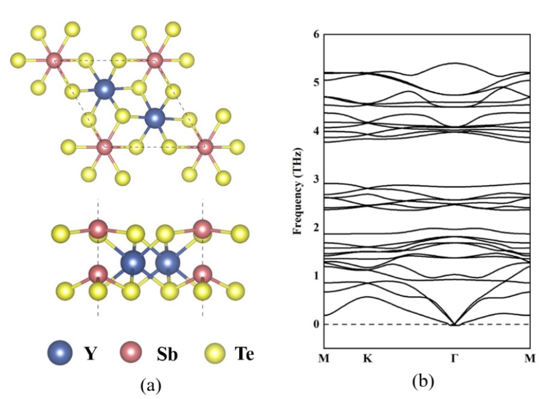
Figure 1. (a) Top and side views of the structure of 2D YSbTe3. The Y, Sb, and Te atoms are represented by blue, red, and yellow balls, respectively. (b) Phonon spectrum of YSbTe3.
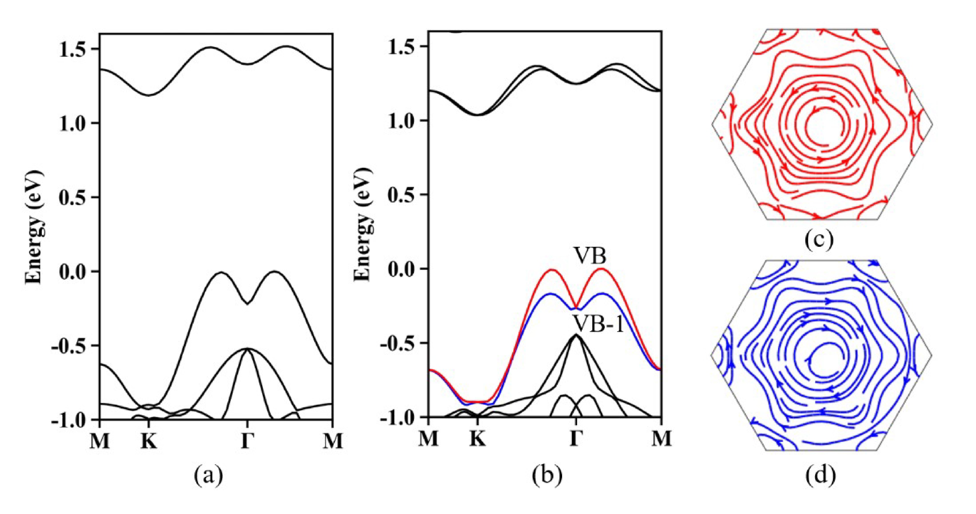
Figure 2. (a, b) Band structures of 2D YSbTe3 calculated with HSE06 and HSE06+SOC, respectively. VB and VB−1 are shown in red and blue, respectively. The characteristic spin texture structures of (c) VB and (d) VB−1 calculated with the HSE06 + SOC functional. The Fermi levels are set to zero.

Figure 3. The relationship between the Rashba constant and the electric field (red line and black dots, left y-axis) and the corresponding electric field response of the Rashba constant (|∆αR/∆E|) (blue line, right y-axis) for 2D YSbTe3.
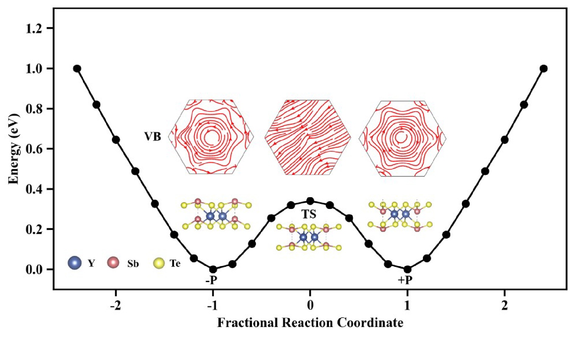
Figure 4. Double-well potential vs. atomic displacement along the z-axis. The energy of the ferroelectric state is taken as a reference. The VB spin textures of two degenerated ferroelectric states and one transition state (TS) are displayed.
| [1] |
Chen J J, Wu K, Hu W, et al. Spin–orbit coupling in 2D semiconductors: a theoretical perspective. J. Phys. Chem. Lett., 2021, 12 (51): 12256–12268. doi: 10.1021/acs.jpclett.1c03662
|
| [2] |
Koo H C, Kim S B, Kim H, et al. Rashba effect in functional spintronic devices. Adv. Mater., 2020, 32 (51): 2002117. doi: 10.1002/adma.202002117
|
| [3] |
Lee S, Koike H, Goto M, et al. Synthetic Rashba spin–orbit system using a silicon metal-oxide semiconductor. Nat. Mater., 2021, 20 (9): 1228–1232. doi: 10.1038/s41563-021-01026-y
|
| [4] |
Lin W, Li L, Doğan F, et al. Interface-based tuning of Rashba spin-orbit interaction in asymmetric oxide heterostructures with 3d electrons. Nat. Commun., 2019, 10 (1): 3052. doi: 10.1038/s41467-019-10961-z
|
| [5] |
Lyu J K, Ji W X, Zhang S F, et al. Strain-tuned topological insulator and Rashba-induced anisotropic momentum-locked Dirac cones in two-dimensional SeTe monolayers. ACS Appl. Mater. Interfaces, 2018, 10 (50): 43962–43969. doi: 10.1021/acsami.8b18582
|
| [6] |
Ciocys S T, Maksimovic N, Analytis J G, et al. Driving ultrafast spin and energy modulation in quantum well states via photo-induced electric fields. npj Quantum Mater., 2022, 7 (1): 79. doi: 10.1038/s41535-022-00490-2
|
| [7] |
Jolie W, Hung T C, Niggli L, et al. Creating tunable quantum corrals on a Rashba surface alloy. ACS Nano, 2022, 16 (3): 4876–4883. doi: 10.1021/acsnano.2c00467
|
| [8] |
Lafalce E, Amerling E, Yu Z G, et al. Rashba splitting in organic–inorganic lead–halide perovskites revealed through two-photon absorption spectroscopy. Nat. Commun., 2022, 13 (1): 483. doi: 10.1038/s41467-022-28127-9
|
| [9] |
Lee S, Kwon Y K. Unveiling giant hidden rashba effects in two-dimensional Si2Bi2. npj 2D Mater. Appl., 2020, 4 (1): 45. doi: 10.1038/s41699-020-00180-2
|
| [10] |
Chen J J, Wu K, Hu W, et al. Tunable Rashba spin splitting in two-dimensional polar perovskites. J. Phys. Chem. Lett., 2021, 12 (7): 1932–1939. doi: 10.1021/acs.jpclett.0c03668
|
| [11] |
Datta S, Das B. Electronic analog of the electro-optic modulator. Appl. Phys. Lett., 1990, 56 (7): 665–667. doi: 10.1063/1.102730
|
| [12] |
Park Y H, Choi J W, Kim H J, et al. Complementary spin transistor using a quantum well channel. Sci. Rep., 2017, 7 (1): 46671. doi: 10.1038/srep46671
|
| [13] |
Chuang P, Ho S C, Smith L W, et al. All-electric all-semiconductor spin field-effect transistors. Nat. Nanotechnol., 2015, 10 (1): 35–39. doi: 10.1038/nnano.2014.296
|
| [14] |
Fu X M, Jia C, Sheng L, et al. Bipolar Rashba semiconductors: a class of nonmagnetic materials for electrical spin manipulation. J. Phys. Chem. Lett., 2023, 14 (50): 11292–11297. doi: 10.1021/acs.jpclett.3c02917
|
| [15] |
Chen J J, Wu K, Hu W, et al. High-throughput inverse design for 2D ferroelectric Rashba semiconductors. J. Am. Chem. Soc., 2022, 144 (43): 20035–20046. doi: 10.1021/jacs.2c08827
|
| [16] |
Song Q, Zhang H R, Su T, et al. Observation of inverse Edelstein effect in Rashba-split 2DEG between SrTiO3 and LaAlO3 at room temperature. Sci. Adv., 2017, 3 (3): e1602312. doi: 10.1126/sciadv.1602312
|
| [17] |
Qu J, Han X, Sakamoto S, et al. Reversal of spin-polarization near the fermi level of the Rashba semiconductor BiTeCl. npj Quantum Mater., 2023, 8 (1): 13. doi: 10.1038/s41535-023-00546-x
|
| [18] |
Nakayama H, Kanno Y, An H, et al. Rashba-Edelstein magnetoresistance in metallic heterostructures. Phys. Rev. Lett., 2016, 117 (11): 116602. doi: 10.1103/PhysRevLett.117.116602
|
| [19] |
Wu K, Chen J J, Ma H H, et al. Two-dimensional giant tunable Rashba semiconductors with two-atom-thick buckled honeycomb structure. Nano Lett., 2021, 21 (1): 740–746. doi: 10.1021/acs.nanolett.0c04429
|
| [20] |
Liu B C, Gao H X, Meng C Y, et al. The impact of an external electric field on the Rashba effect in two-dimensional hybrid perovskites. J. Mater. Chem. C, 2023, 11 (30): 10370–10376. doi: 10.1039/D3TC01575K
|
| [21] |
Kresse G, Furthmüller J. Efficient iterative schemes for ab initio total-energy calculations using a plane-wave basis set. Phys. Rev. B, 1996, 54 (16): 11169–11186. doi: 10.1103/PhysRevB.54.11169
|
| [22] |
Blöchl P E. Projector augmented-wave method. Phys. Rev. B, 1994, 50 (24): 17953–17979. doi: 10.1103/PhysRevB.50.17953
|
| [23] |
Perdew J P, Burke K, Ernzerhof M. Generalized gradient approximation made simple. Phys. Rev. Lett., 1996, 77 (18): 3865–3868. doi: 10.1103/PhysRevLett.77.3865
|
| [24] |
Grimme S, Antony J, Ehrlich S, et al. A consistent and accurate ab initio parametrization of density functional dispersion correction (DFT-D) for the 94 elements H-Pu. J. Chem. Phys., 2010, 132 (15): 154104. doi: 10.1063/1.3382344
|
| [25] |
Heyd J, Scuseria G E, Ernzerhof M. Hybrid functionals based on a screened Coulomb potential. J. Chem. Phys., 2003, 118 (18): 8207–8215. doi: 10.1063/1.1564060
|
| [26] |
Alfè D. PHON: A program to calculate phonons using the small displacement method. Comput. Phys. Commun., 2009, 180 (12): 2622–2633. doi: 10.1016/j.cpc.2009.03.010
|
| [27] |
Togo A, Chaput L, Tadano T, et al. Implementation strategies in phonopy and phono3py. J. Phys. : Condens. Matter, 2023, 35 (35): 353001. doi: 10.1088/1361-648X/acd831
|
| [28] |
Sheppard D, Xiao P, Chemelewski W, et al. A generalized solid-state nudged elastic band method. J. Chem. Phys., 2012, 136 (7): 074103. doi: 10.1063/1.3684549
|
| [29] |
Ali M S, Das S, Abed Y F, et al. Lead-free CsSnCl3 perovskite nanocrystals: rapid synthesis, experimental characterization and DFT simulations. Phys. Chem. Chem. Phys., 2021, 23 (38): 22184–22198. doi: 10.1039/D1CP02666F
|
| [30] |
Bahramy M S, Arita R, Nagaosa N. Origin of giant bulk Rashba splitting: Application to BiTeI. Phys. Rev. B, 2011, 84 (4): 041202. doi: 10.1103/PhysRevB.84.041202
|
| [31] |
Gupta S, Yakobson B I. What dictates Rashba splitting in 2D van der Waals heterobilayers. J. Am. Chem. Soc., 2021, 143 (9): 3503–3508. doi: 10.1021/jacs.0c12809
|
| [32] |
Wu Q, Cao L, Ang Y S, et al. Semiconductor-to-metal transition in bilayer MoSi2N4 and WSi2N4 with strain and electric field. Appl. Phys. Lett., 2021, 118 (11): 113102. doi: 10.1063/5.0044431
|
| [33] |
Nourbakhsh A, Agarwal T K, Klekachev A, et al. Chemically enhanced double-gate bilayer graphene field-effect transistor with neutral channel for logic applications. Nanotechnology, 2014, 25 (34): 345203. doi: 10.1088/0957-4484/25/34/345203
|

ISSN 0253-2778
CN 34-1054/N
Copyright © Editorial Office of JUSTC, All Rights Reserved. 皖ICP备05002528号
Supported by:
Beijing Renhe Information Technology Co. Ltd


 DownLoad: